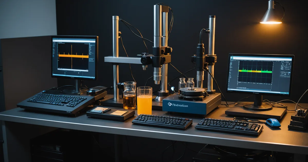
The NV-center sensor performance we specify starts with the diamond chip, and the diamond chip starts with how the material is grown. This post covers the key steps from CVD growth through nitrogen implantation and annealing to the finished chip we install in the sensor head, and the manufacturing constraints that create variability in the final product. We are not the only group working on this; much of the underlying materials science is published research. But the path from published method to reliable instrument-grade chip involves engineering decisions that aren't always described in papers.
CVD diamond growth: the purity baseline
Chemical vapour deposition (CVD) diamond is grown from a hydrogen and methane plasma on a substrate, typically a high-pressure high-temperature (HPHT) diamond seed. The quality parameters that matter for NV-center magnetometry are nitrogen concentration in the as-grown crystal and the presence of other paramagnetic impurities, primarily substitutional nitrogen (the P1 centre) and silicon-vacancy defects introduced from etching chemistry or reactor wall contamination.
For ensemble NV-center magnetometry, a nitrogen concentration in the range of 10 to 100 parts per billion nitrogen in the as-grown crystal is the starting point. Too low, and there isn't enough precursor nitrogen for efficient NV creation after implantation. Too high, and P1 centre spin bath density increases, reducing the NV coherence time T2 and thus sensitivity. The growth nitrogen concentration must be controlled to approximately factor-of-two accuracy to keep the final NV and P1 concentrations in the target range.
We source our diamond substrates from two suppliers who have demonstrated consistent nitrogen control in this range, verified by secondary ion mass spectrometry (SIMS) analysis of each wafer batch. This adds cost and lead time relative to using off-the-shelf CVD diamond, but inconsistent substrate quality produces sensors with variable T2, which produces variable sensitivity that is difficult to screen for without testing every chip. We learned this the hard way in our first year of operation, when a batch of sensors from a single supplier lot showed T2 scatter of more than a factor of three across chips.
Nitrogen implantation and vacancy creation
Nitrogen-vacancy centers are created by ion implantation of nitrogen ions into the diamond crystal, followed by high-temperature annealing. The implantation energy determines the depth profile of the implanted nitrogen, and the fluence determines the surface density of implanted atoms. After implantation, the diamond contains implanted nitrogen and implantation damage (lattice vacancies and interstitials). Annealing at 800 to 1000 degrees Celsius in vacuum allows the vacancies to migrate and combine with the implanted nitrogen to form NV centers.
The conversion efficiency from implanted nitrogen to NV center is typically 1 to 10 percent under conditions optimised for ensemble sensing. The remaining implanted nitrogen becomes P1 centres, which contribute to the spin bath. Improving conversion efficiency is an active research area; higher efficiency would allow lower total implantation dose while achieving the same NV density, reducing the P1 spin bath and improving T2. We are currently achieving approximately 5 percent conversion efficiency with our standard protocol, consistent with published results from comparable facilities.
Implantation damage also affects T2 even after annealing. Complete healing of the lattice requires careful thermal cycling and is sensitive to annealing atmosphere. In our process, we achieve a post-anneal T2 of 15 to 50 microseconds across the implanted layer, with chip-to-chip variation of approximately 30 percent. This T2 range is the dominant source of sensor-to-sensor sensitivity variation in our current production.
Surface preparation and optical coating
The photoluminescence collection efficiency from the NV layer depends on the surface quality of the diamond chip and the optical coupling geometry. A polished surface with roughness below 5 nanometres Ra allows the highest collection efficiency through the directly bonded objective. Rougher surfaces scatter light and reduce the detected photon flux, degrading sensitivity.
We apply an anti-reflection coating at 532 nm (pump laser wavelength) to the pump entry face and an anti-reflection coating at 637 to 750 nm (NV emission band) to the collection face. These coatings are standard thin-film evaporation deposited on the polished diamond by our optics supplier. Each coated chip is inspected for coating uniformity before assembly. Chips with coating non-uniformity above 5 percent across the active area are rejected.
The current yield through the full process from substrate to inspection-passed chip is approximately 60 percent, with the main loss modes being polishing damage (18 percent loss), coating non-uniformity (11 percent loss), and T2 below specification (11 percent loss). This 60 percent yield determines the effective cost of our sensor chips and is a primary driver of instrument cost. Improving yield from 60 to 80 percent would reduce chip cost by approximately 25 percent at current processing volumes, which is a meaningful target for the next development phase.
Microwave antenna integration
The NV spin resonance must be driven by a microwave field at approximately 2.87 GHz. In our sensor design, this is delivered by a thin-film copper antenna pattern deposited directly on the diamond chip surface, adjacent to the NV layer. The antenna geometry is designed to maximise microwave field uniformity across the NV ensemble volume while minimising resistive heating, which would create a local temperature gradient that drives resonance frequency shift during operation.
The antenna is fabricated by photolithography and electroplating on the polished diamond surface, using a process adapted from thin-film MEMS fabrication. Line widths are 20 to 50 micrometres, and the completed antenna adds approximately 2 micrometres of thickness to the chip surface. Bonding the antenna chip into the sensor head requires careful alignment of the antenna feed pads to the RF connector in the housing, which is done under a microscope during final assembly.
The manufacturing readiness gap
Every step described above can produce high-quality chips in small quantities under controlled conditions. The gap between "can produce" and "reliably produce at scale" is where early-stage hardware companies spend most of their time. Our current production cadence is approximately 20 sensor chips per quarter, which is adequate for internal development and evaluation kit deployment but is not a manufacturing operation in any meaningful sense.
Moving to a contracted manufacturing model, where a qualified external fab performs the implantation and annealing steps to our specification, is a development we have scoped but not yet executed. The primary technical barrier is transferring our annealing protocol to a facility with different furnace geometry and atmosphere control, without degrading T2 consistency. This qualification work is planned for later this year and will be a prerequisite for any increase in production volume.
Contact Dr. Chen Wei to discuss the materials specifications and what constraints they create for specific measurement applications.
Contact the Team