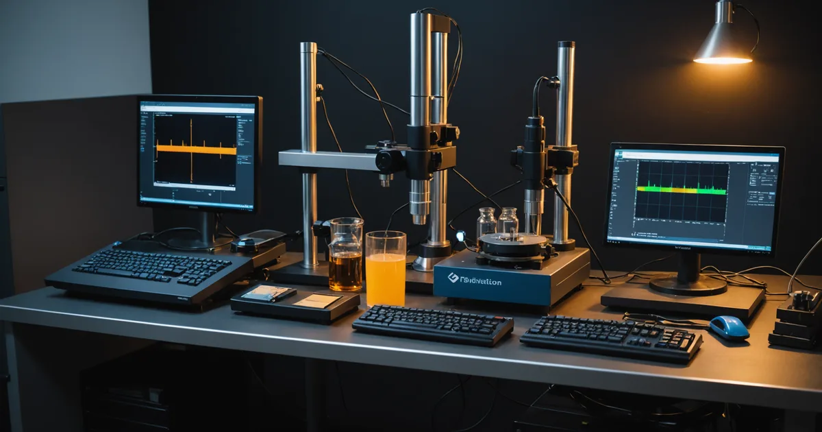
We started DeteQt in early 2023. At that point, James Rabeau had spent years in academic NV-center quantum optics research, and Dr. Chen Wei had a background in diamond materials processing and photonic device fabrication. The question we were trying to answer was not "can we build an NV-center magnetometer" (that had been demonstrated in labs many times) but "can we build one that works reliably outside a controlled lab environment, and can we do it from Sydney." This is an account of what we have found out over two years, not a pitch for the technology or the city.
The fabrication access problem
Deep-tech hardware in the quantum sensing domain requires specialist fabrication capabilities that are concentrated in a small number of locations globally: diamond CVD growth facilities, ion implantation facilities capable of precisely controlled shallow nitrogen implantation at the right energy and fluence, thin-film deposition for optical coatings, and clean-room photolithography for microwave antenna patterning. None of these are in Sydney. The nearest ion implantation facility we have worked with is in Japan. Our diamond CVD substrates come from European suppliers. Our optical coatings come from a specialist thin-film house in the UK.
This creates a supply chain that is geographically stretched in a way that software companies do not experience and that even conventional hardware companies building products from standard electronic components do not face. Each cycle of "design, fabricate, characterise, modify" takes weeks to months for the diamond chip steps alone, where a software cycle takes hours. The practical consequence is that iteration speed is a function of how well you have specified the next experiment before you need to order the materials, and how many parallel experiments you can run with limited chip inventory.
After two years, we have settled into a workable rhythm: two implantation runs per year at the Japanese facility, with each run producing enough chips for six months of instrument builds and experiments. The 6-month horizon forces better planning than a shorter cycle would, but it also means that when something unexpected happens in a characterisation run, the next opportunity to test a modified specification is months away.
Talent and the university pipeline
Sydney has a strong physics department ecosystem, and the quantum sensing field has developed enough that graduates with relevant background (quantum optics, diamond photonics, precision measurement) are coming out of Australian universities at a rate that was not true five years ago. We have been able to hire people with directly relevant doctoral research backgrounds from UNSW and Macquarie, which would not have been straightforward in 2019.
The talent situation for the signal processing side of the work is more straightforward: applied mathematics and machine learning graduates are plentiful in Sydney, and the specific problem of ODMR signal deconvolution is not so exotic that only people with NV-center backgrounds can work on it. Dr. Priya Nair joined from a computational neuroscience background rather than from quantum sensing, and that turned out to be an advantage: the signal recovery problem in NV magnetometry has structural similarities to the neural source localisation problem in MEG, and her intuition about the geometry of the deconvolution problem was directly applicable.
The physics-to-engineering translation gap
Academic quantum sensing papers are almost always about a specific physics result achieved under optimal conditions: low temperature, controlled vibration environment, no RF interference, unlimited time for signal averaging. The engineering challenge is to achieve a useful fraction of that result under field conditions with a constrained budget for size, weight, power, and cost. This gap is not specific to Australia or Sydney; it exists everywhere quantum instruments are being commercialised. But it is worth being explicit about, because it determines how much development time separates a laboratory demonstration from a field-deployable product.
In our case, the initial lab version of the instrument achieved 15 to 20 pT per root hertz in a quiet room. The first field prototype that we could carry to a survey site achieved 120 pT per root hertz under survey conditions. The current generation achieves 50 to 80 pT per root hertz in field conditions. That progression from 15 to 120 to 50 to 80 took roughly 18 months of engineering work on packaging, vibration isolation, thermal management, and signal processing. The underlying physics did not change; the work was almost entirely engineering.
We are not the first team to navigate this gap, and the academic literature on field-deployable quantum sensors is more extensive than it was five years ago. But the literature is still skewed toward reporting laboratory performance, and the engineering work of field deployment is underrepresented. Early-stage hardware companies in this space spend a larger fraction of their time on this translation work than they typically expect when they start.
Access to field test environments
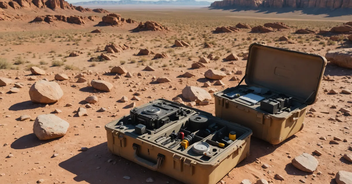
One genuine advantage of building this technology in Australia, and specifically with a mining application in view, is proximity to exploration programs where field testing is possible. The WA mining industry operates at a scale and density that is unusual globally, and the willingness of exploration companies to run evaluation pilots with new survey instrumentation is higher than we expected. Our first real field deployment came from an introduction through the mining industry network in Perth, not through any formal commercialisation pathway.
This access has been important for development. Every field deployment has returned data that revealed a limitation we had not characterised in the lab, and fixing those limitations has occupied a significant fraction of development time. The feedback loop between field observation and lab improvement is the primary mechanism by which the field performance of the instrument has improved. Access to that feedback loop early is worth more than a larger lab budget in some respects.
What we wish we had known at the start
The lead times on specialist fabrication steps are long and compound. Parallel-pathing experiments and building more buffer inventory than feels necessary is consistently worth it. The physics-to-engineering gap is wider than academic papers suggest and narrower than it sometimes feels during debugging. Field testing access can be found earlier in development than it seems like it should be, and the cost of a failed field pilot is lower than the cost of missing six months of field feedback by waiting until the instrument is "ready." Australia is not the optimal location for every piece of the supply chain, but it is workable, and proximity to the mining industry creates a field testing advantage that compensates substantially for the fabrication geography.
We want to be direct about what this account covers and what it does not: these are observations from one team at one company over two years of a specific technology in a specific market. Deep-tech hardware in different domains (MEMS sensors, photonic devices, quantum computing) will share some of these dynamics and differ in others. We are not making a general claim about Sydney as a hardware hub, just reporting what has been true for this problem in this period.
If you are working on quantum sensing applications in mining or medical imaging and want to discuss technical collaboration or evaluation, contact us directly.
Request Evaluation Kit